NVIDIA Blackwell
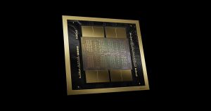
NVIDIA Blackwell is a GPU architecture and data center platform family by NVIDIA introduced on March 18, 2024 at the company's Graphics Technology Conference (GTC). It succeeds NVIDIA Hopper for datacenter and Ada Lovelace for consumer graphics, and underpins products such as the B200 Tensor Core GPU, the GB200 Grace Blackwell Superchip (which couples two B200 GPUs with a Grace CPU), rack-scale systems like GB200 NVL72, and the consumer GeForce RTX 50 series. Blackwell-architecture GPUs comprise two reticle-limited dies linked by a 10 TB/s chip-to-chip interconnect in a single logical GPU, are fabricated on custom TSMC 4NP for datacenter and 4N for consumer products, and pack 208 billion transistors in datacenter variants.[1]
History and Naming
The architecture was first leaked in 2022, with the B40 and B100 accelerators confirmed in October 2023 via an official NVIDIA roadmap during an investors' presentation when "Hopper-Next" was replaced with "Blackwell".[2] NVIDIA CEO Jensen Huang officially announced Blackwell at GTC 2024, stating the company invested approximately $10 billion in research and development for the NV-HBI die interconnect technology.[2]
Blackwell is named after David Harold Blackwell (1919–2010), an American statistician and mathematician who was the first Black scholar elected to the U.S. National Academy of Sciences in 1965 and the first Black tenured faculty member at the University of California, Berkeley. His contributions to game theory, probability theory, information theory, and statistics—including the Rao-Blackwell theorem—have influenced modern artificial intelligence and machine learning algorithms that form the foundation of today's AI systems.[3][4]
Key architectural features
- Dual-die, single-GPU design. All Blackwell-architecture datacenter GPUs consist of two reticle-limited dies (GB100, each with 104 billion transistors) connected internally by a 10 TB/s NV-High Bandwidth Interface (NV-HBI) based on NVLink 7 protocol, presented as one GPU to software with full cache coherency.[1][2]
- Second-generation Transformer Engine. Adds micro-tensor scaling and community-defined microscaling formats (MXFP4, MXFP6), enabling FP4 inference and larger effective model sizes while maintaining accuracy; acceleration for attention layers is increased versus prior generation. Includes CUDA Compute Capability 10.x/12.x support.[1][3]
- Fifth-generation NVLink. Up to 1.8 TB/s bidirectional throughput per GPU (18 NVLink5 links at 100 GB/s each) and scale-up to 576 GPUs; the NVLink Switch Chip enables a 72-GPU NVLink domain with 130 TB/s aggregate GPU bandwidth (NVL72).[3][1]
- Fifth-generation Tensor Cores. Support for new precision formats including FP4 (4-bit floating point), FP6, FP8, FP16, BF16, TF32, FP32, and FP64 operations for enhanced AI and HPC workloads.[5]
- Fourth-generation RT Cores (consumer). Feature Triangle Cluster Intersection Engine for mega geometry and Linear Swept Spheres for fine details like hair, with 2× ray-triangle intersection throughput.[2]
- AI Management Processor (AMP). RISC-V-based dedicated scheduler chip on the GPU that offloads scheduling from the CPU, improving resource control via Windows Hardware-Accelerated GPU Scheduling (HAGS).[2]
- Confidential computing ("Secure AI"). First TEE-I/O capable GPU family with inline protection over NVLink, offering near-parity throughput to unencrypted modes when paired with compatible hosts; supports protected paging and encryption mechanisms for model/data isolation.[1][6]
- RAS Engine. Dedicated hardware for reliability, availability, and serviceability with AI-based predictive management to minimize downtime at hyperscale.[1]
- Decompression engine. Hardware acceleration for formats such as LZ4, Snappy and Deflate at 800 GB/s to speed database/analytics pipelines; tightly coupled with Grace CPU over 900 GB/s NVLink-C2C.[1][3]
Products
Datacenter Products
B200 and B100 Tensor Core GPUs
The B200 is the flagship Blackwell data center GPU used standalone (for example HGX B200 8-GPU servers) and within GB200 Grace Blackwell Superchip. The B100 is a lower-power variant with 700W TDP designed for drop-in compatibility with existing H100 infrastructure. Both feature two GB100 dies with 208 billion total transistors and 192 GB HBM3e memory with 8 TB/s bandwidth.[3][7]
GB200 Grace Blackwell Superchip
The GB200 Grace Blackwell Superchip integrates one Grace CPU with two B200 GPUs over NVLink-C2C (900 GB/s bidirectional), providing a tightly coupled CPU-GPU memory system with 864 GB total unified memory for large-scale LLM workloads.[3]
Blackwell Ultra (GB300 generation)
In 2025, NVIDIA introduced "Blackwell Ultra," including GB300 NVL72, targeting order-of-magnitude gains in AI reasoning and real-time generation compared to NVIDIA Hopper.[1][8]
Rack-scale systems
GB200 NVL72
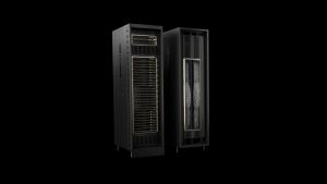
The GB200 NVL72 connects 36 GB200 Grace Blackwell Superchips (72 B200 GPUs + 36 Grace CPUs) in a liquid-cooled rack with a single 72-GPU NVLink domain that behaves like one giant GPU for software. System power consumption is approximately 120kW.[9]
| Metric | GB200 NVL72 (rack) | GB200 Grace Blackwell Superchip (per node) |
|---|---|---|
| FP4 Tensor Core (with sparsity) | 1,440 PFLOPS | 40 PFLOPS |
| FP8/FP6 Tensor Core (with sparsity) | 720 PFLOPS | 20 PFLOPS |
| INT8 Tensor Core (with sparsity) | 720 POPS | 20 POPS |
| FP16/BF16 Tensor Core (with sparsity) | 360 PFLOPS | 10 PFLOPS |
| TF32 Tensor Core | 180 PFLOPS | 5 PFLOPS |
| FP32 | 5,760 TFLOPS | 160 TFLOPS |
| FP64 / FP64 Tensor Core | 2,880 TFLOPS | 80 TFLOPS |
| GPU memory (HBM3e) | Up to 13.4 TB, 576 TB/s | Up to 372 GB, 16 TB/s |
| NVLink bandwidth | 130 TB/s | 3.6 TB/s |
| CPU cores (Arm Neoverse V2) | 2,592 | 72 |
| CPU memory (LPDDR5X) | Up to 17 TB, up to 18.4 TB/s | Up to 480 GB, up to 512 GB/s |
Consumer Products (GeForce RTX 50 Series)
The GeForce RTX 50 series based on Blackwell architecture was announced at CES 2025 on January 6, 2025. Consumer dies use TSMC 4N process and do not feature the dual-die design of datacenter parts.[11]
| Model | GPU | CUDA Cores | Memory | Bus Width | Die Size | Transistors | TDP | MSRP | Release Date |
|---|---|---|---|---|---|---|---|---|---|
| RTX 5090 | GB202-300-A1 | 21,760 | 32 GB GDDR7 | 512-bit | 750 mm² | 92.2 bn | 575W | $1,999 | January 30, 2025 |
| RTX 5080 | GB203-200-A1 | 10,752 | 16 GB GDDR7 | 256-bit | 378 mm² | 45.6 bn | 360W | $999 | January 30, 2025 |
| RTX 5070 Ti | GB203-300-A1 | 8,960 | 16 GB GDDR7 | 256-bit | 378 mm² | 45.6 bn | 300W | $749 | February 2025 |
| RTX 5070 | GB205-300-A1 | 6,144 | 12 GB GDDR7 | 192-bit | 263 mm² | 31.1 bn | 250W | $549 | February 2025 |
Professional RTX PRO Blackwell series includes RTX PRO 6000 (96 GB VRAM, April 2025) and RTX PRO 5000/4500/4000 (summer 2025).[13]
Comparison to Previous Generation
| Feature | NVIDIA H100 | NVIDIA B200 (Blackwell) |
|---|---|---|
| Transistors | 80 Billion | 208 Billion (dual-die) |
| Process Node | TSMC 4N | TSMC 4NP |
| Max AI Performance | 4 PFLOPS (FP8) | 20 PFLOPS (FP4) / 10 PFLOPS (FP8) |
| Max GPU Memory | 80 GB HBM3 | 192 GB HBM3e |
| Memory Bandwidth | 3.35 TB/s | 8 TB/s |
| NVLink (GPU-to-GPU) | 4th Gen: 900 GB/s | 5th Gen: 1.8 TB/s |
| TDP | 700W | 1000W |
Software, networking, and platforms
Blackwell systems are offered in HGX and DGX platforms, and as managed DGX Cloud instances, and pair with NVIDIA's Quantum-X800 InfiniBand and Spectrum-X Ethernet fabrics (up to 800 Gb/s) and BlueField-3 DPUs for secure, composable acceleration.[3] NVIDIA AI Enterprise includes NVIDIA NIM inference microservices for Blackwell deployment.[1]
Performance claims
At announcement, NVIDIA stated that, per chip, Blackwell delivers:
- Up to 2.5× the FP8 training throughput of NVIDIA Hopper
- Up to 5× the inference performance at FP4
- 30× faster real-time trillion-parameter LLM inference (NVL72 vs H100 cluster)
- 4× faster LLM training at massive scale
- 25× improvement in cost and energy efficiency for trillion-parameter models
- 18× faster database query performance compared to CPUs[3][10]
Market Reception and Future Roadmap
By November 2024, Morgan Stanley reported that the entire 2025 production of Blackwell was sold out. Major cloud providers including Amazon Web Services, Google, Meta, Microsoft, OpenAI, Oracle, and Tesla have committed to adopting Blackwell-based systems.[2]
Initial consumer RTX 50 series availability faced supply constraints, with some units found missing eight render output units (ROPs) due to a "production anomaly" affecting less than 0.5% of cards according to NVIDIA.[15]
NVIDIA's roadmap includes Blackwell Ultra enhancements in 2025, followed by the Vera Rubin architecture (comprised of Rubin GPU and Vera CPU) scheduled for 2026 with HBM4 memory.[8]
See also
- NVIDIA Hopper
- Ada Lovelace (microarchitecture)
- Grace CPU
- NVLink
- GeForce RTX 50 series
- Tensor Core
- David Blackwell
- DGX SuperPOD
- DLSS
References
- ↑ 1.0 1.1 1.2 1.3 1.4 1.5 1.6 1.7 1.8 https://www.nvidia.com/en-us/data-center/technologies/blackwell-architecture/ — NVIDIA Blackwell Architecture: official technology page with manufacturing node, dual-die design, transistor count; second-gen Transformer Engine; fifth-gen NVLink scale; NVLink Switch (130 TB/s NVL72 domain); Secure AI/Confidential Computing; RAS; Decompression engine.
- ↑ 2.0 2.1 2.2 2.3 2.4 2.5 https://en.wikipedia.org/wiki/Blackwell_(microarchitecture) — Blackwell (microarchitecture) Wikipedia entry: historical timeline, technical specifications, market reception.
- ↑ 3.0 3.1 3.2 3.3 3.4 3.5 3.6 3.7 https://nvidianews.nvidia.com/news/nvidia-blackwell-platform-arrives-to-power-a-new-era-of-computing — NVIDIA Newsroom (Mar 18, 2024): Blackwell platform launch; GB200 Grace Blackwell Superchip overview; NVLink-C2C 900 GB/s; NVLink throughput per GPU; NVL72 topology and performance positioning; partner/availability context; naming origin.
- ↑ https://en.wikipedia.org/wiki/David_Blackwell — David Blackwell biography and contributions to mathematics and statistics.
- ↑ https://www.nvidia.com/en-us/data-center/tensor-cores/ — Tensor Cores: Versatility for HPC & AI, NVIDIA official page.
- ↑ https://docs.nvidia.com/nvidia-secure-ai-with-blackwell-and-hopper-gpus-whitepaper.pdf — NVIDIA Whitepaper (Aug 14, 2025): "NVIDIA Secure AI with Blackwell and Hopper GPUs" discussing Blackwell B100/B200 confidential computing, protected paging, and TEE-I/O context.
- ↑ 7.0 7.1 https://www.amax.com/comparing-nvidia-blackwell-configurations/ — AMAX (Mar 26, 2024): Comparing NVIDIA Blackwell Configurations: GB200, B200, B100 specifications.
- ↑ 8.0 8.1 https://www.theverge.com/news/631835/nvidia-blackwell-ultra-ai-chip-gb300 — The Verge (Mar 2025): coverage of Blackwell Ultra/GB300 family timing and positioning; future Vera Rubin architecture.
- ↑ https://www.fibermall.com/blog/nvidia-gb200-superchip.htm — Fibermall (Oct 12, 2024): Introduction to NVIDIA GB200 Superchip and Liquid-Cooled Servers and Cabinets, power consumption details.
- ↑ 10.0 10.1 https://www.nvidia.com/en-us/data-center/gb200-nvl72/ — NVIDIA GB200 NVL72 product page: official specifications table (PFLOPS/POPS by precision with sparsity notes), HBM3e capacities and bandwidths, NVLink domain bandwidth, CPU core counts and LPDDR5X capacities, and system claims (30× inference, 4× training, 25× efficiency vs. H100).
- ↑ https://www.videocardz.com/newz/nvidia-launches-geforce-rtx-50-blackwell-series — VideoCardz (Jan 7, 2025): NVIDIA launches GeForce RTX 50 "Blackwell" series announcement details.
- ↑ https://en.wikipedia.org/wiki/GeForce_RTX_50_series — GeForce RTX 50 series Wikipedia entry with specifications and release dates.
- ↑ https://www.cgchannel.com/2025/03/nvidia-unveils-blackwell-rtx-pro-gpus-with-up-to-96gb-vram/ — CG Channel: NVIDIA unveils Blackwell RTX PRO GPUs professional lineup.
- ↑ https://www.aventusinformatics.com/blog_details/nvidia-blackwell-vs-hopper-a-leap-in-ai-training-performance — Aventus Informatics (Oct 12, 2025): Nvidia Blackwell vs. Hopper performance comparison.
- ↑ https://en.wikipedia.org/wiki/GeForce_RTX_50_series — GeForce RTX 50 series production anomaly information.


