NVIDIA Blackwell
Last edited
Fact-checked
In review queue
Sources
33 citations
Revision
v14 · 6,442 words
Fact-checks are independent of edits: a reviewer re-verifies the article against its sources and stamps the date. How we verify
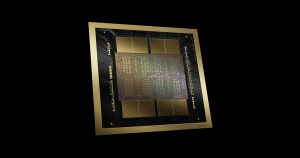
NVIDIA Blackwell is the data center and consumer GPU architecture NVIDIA unveiled on March 18, 2024 to power trillion-parameter AI, built from two reticle-limited dies fused into one logical GPU with 208 billion transistors, a second-generation Transformer Engine with FP4 precision, and fifth-generation NVLink. It is a GPU architecture and data center platform family by NVIDIA introduced at the company's Graphics Technology Conference (GTC). It succeeds NVIDIA Hopper for datacenter and Ada Lovelace for consumer graphics, and underpins products such as the B200 Tensor Core GPU, the GB200 Grace Blackwell Superchip (which couples two B200 GPUs with a Grace CPU), rack-scale systems like GB200 NVL72 and the Blackwell Ultra GB300 NVL72, and the consumer GeForce RTX 50 series. Blackwell-architecture GPUs comprise two reticle-limited dies linked by a 10 TB/s chip-to-chip interconnect in a single logical GPU, are fabricated on custom TSMC 4NP for datacenter and 4N for consumer products, and pack 208 billion transistors in datacenter variants.[1]
With its dual-die design, second-generation Transformer Engine supporting FP4 precision, and fifth-generation NVLink interconnect, Blackwell represents a generational leap in AI compute density. NVIDIA has described Blackwell as the engine behind "AI factories," positioning the architecture as the foundation for training and deploying trillion-parameter large language models. By Q2 of NVIDIA's fiscal year 2026 (ending July 27, 2025), Blackwell contributed roughly 70% of datacenter compute revenue and Blackwell datacenter revenue grew 17% sequentially, with the architecture sold out through mid-2026.[18][19] By NVIDIA's fourth quarter of fiscal 2026 (ended January 25, 2026), data center revenue reached a record $62.3 billion in a single quarter, up 75% year over year, with CEO Jensen Huang stating that "Grace Blackwell with NVLink is the king of inference today."[29]
When was NVIDIA Blackwell released, and how is it named?
The architecture was first leaked in 2022, with the B40 and B100 accelerators confirmed in October 2023 via an official NVIDIA roadmap during an investors' presentation when "Hopper-Next" was replaced with "Blackwell".[2] NVIDIA CEO Jensen Huang officially announced Blackwell at GTC 2024, stating the company invested approximately $10 billion in research and development for the NV-HBI die interconnect technology.[2]
David Harold Blackwell
Blackwell is named after David Harold Blackwell (April 24, 1919 to July 8, 2010), an American statistician and mathematician whose work profoundly influenced the fields that underpin modern artificial intelligence. Born in Centralia, Illinois, Blackwell showed exceptional mathematical talent from a young age. His passion for mathematics began during a high school geometry course, and he graduated from high school in 1935 at the age of sixteen.[3][4]
Blackwell earned his Bachelor of Arts (1938), Master of Arts (1939), and Ph.D. (1941) from the University of Illinois at Urbana-Champaign, completing his doctoral dissertation on Markov chains under the supervision of Joseph L. Doob. At the time, he was only the seventh African American to earn a Ph.D. in mathematics in the United States. He joined the faculty of Howard University in 1944, where he served as Head of the Mathematics Department from 1947 to 1954.[3][4]
In 1954, Blackwell was recruited to the University of California, Berkeley, where he became the institution's first African American tenured professor. He also served as chairman of Berkeley's statistics department from 1957 to 1961. In 1965, Blackwell became the first African American scholar elected to the U.S. National Academy of Sciences.[3][4]
Blackwell made foundational contributions to game theory, probability theory, information theory, and Bayesian statistics. He is known for the Rao-Blackwell theorem, a fundamental result in mathematical statistics that provides a method for improving estimators. He independently developed key ideas in dynamic programming, which finds applications today in finance, genomic analysis, and reinforcement learning algorithms. His 1954 book Theory of Games and Statistical Decisions, co-authored with Abraham Girshick, became a landmark text. During his time as a consultant at the RAND Corporation (1948 to 1950), Blackwell applied game theory to military strategy by modeling the optimal timing of theoretical armed duels.[3][4]
Blackwell was posthumously awarded the National Medal of Science in 2012. Numerous mathematical concepts and awards bear his name, including Blackwell games, Blackwell determinacy, and the MAA-NAM David Blackwell Lecture. His contributions to game theory, probability theory, and statistics have influenced the machine learning and deep learning algorithms that form the backbone of today's AI systems.
Architecture
Dual-Die Design
All Blackwell-architecture datacenter GPUs consist of two reticle-limited dies (codenamed GB100, each with 104 billion transistors for a total of 208 billion) connected internally by a 10 TB/s NV-High Bandwidth Interface (NV-HBI) based on NVLink 7 protocol. The two dies are presented as one GPU to software with full cache coherency.[1][2] This approach was necessary because the transistor count required for Blackwell exceeded the maximum size of a single reticle on TSMC's lithography equipment. The NV-HBI interconnect operates at 10 TB/s bidirectional bandwidth, allowing the two dies to communicate with latency low enough that workloads see a single unified GPU.
The datacenter B200 GPU enables 148 streaming multiprocessors (SMs) across both dies (74 per die out of 80 physical SMs, with some disabled for yield), providing approximately 18,432 CUDA cores and 592 fifth-generation Tensor Cores. Each SM offers 228 KB of shared memory with 64 concurrent warps to maximize utilization.[5][6]
The B200 is fabricated on TSMC's custom 4NP process node, an optimized variant of the 4 nm class process developed in collaboration with NVIDIA specifically for high-performance datacenter chips. Consumer Blackwell products (GeForce RTX 50 series) use the standard TSMC 4N process and feature monolithic (single-die) designs rather than the dual-die approach of datacenter parts.[2]
Second-Generation Transformer Engine
The second-generation Transformer Engine is one of Blackwell's most significant innovations. It adds micro-tensor scaling and community-defined microscaling formats (MXFP4, MXFP6), enabling FP4 inference and larger effective model sizes while maintaining accuracy. Blackwell Ultra further introduces NVFP4, an NVIDIA-defined 4-bit floating-point format whose two-level micro-scaling (FP8 block scale plus FP32 tensor scale) targets near-FP8 accuracy while delivering FP4 throughput; native NVFP4 support is provided in TensorRT-LLM, SGLang, and vLLM with kernels optimized for the dual-die architecture.[20] By operating at 4-bit floating-point precision, Blackwell can effectively double the model size that fits in GPU memory compared to 8-bit formats, while also doubling throughput for inference workloads.[1][3]
The Transformer Engine dynamically adjusts precision during computation, using higher precision where needed for accuracy and lower precision where performance gains can be achieved without sacrificing output quality. This approach is particularly effective for large language model inference, where many layers and operations can tolerate reduced precision without measurable degradation in response quality.
Blackwell's Tensor Cores support a wide range of precision formats:
| Precision Format | Use Case | Blackwell Support |
|---|---|---|
| NVFP4 | Reasoning inference, low-precision training | New in Blackwell Ultra |
| FP4 (MXFP4) | Inference, lightweight training | New in Blackwell |
| FP6 | Inference with higher accuracy | New in Blackwell |
| FP8 | Training and inference | Enhanced from Hopper |
| FP16 / BF16 | Standard mixed-precision training | Yes |
| TF32 | Drop-in replacement for FP32 training | Yes |
| FP32 | High-precision compute | Yes |
| FP64 | Scientific/HPC workloads | Yes |
| INT8 | Quantized inference | Yes |
Fifth-Generation NVLink
Blackwell introduces fifth-generation NVLink, delivering up to 1.8 TB/s bidirectional throughput per GPU through 18 NVLink5 links running at 100 GB/s each. This represents more than 14 times the bandwidth of PCIe Gen5 and double the per-GPU NVLink bandwidth of the Hopper H100.[1][3]
The NVLink Switch Chip is a dedicated ASIC that enables all-to-all GPU communication within a rack-scale domain. In the GB200 NVL72 configuration, nine NVLink Switch chips route traffic between all 72 GPUs, creating a 130 TB/s aggregate bandwidth domain with approximately 300 nanosecond switch latency. Each NVLink switch tray provides 144 NVLink ports, fully connecting all 18 NVLink ports on every one of the 72 Blackwell GPUs.[1][7]
For even larger deployments, the fifth-generation NVLink architecture can scale up to 576 GPUs in a single NVLink domain with over 1 PB/s total bandwidth, enabling efficient training of trillion-parameter and multi-trillion-parameter AI models without requiring slower fabric interconnects for GPU-to-GPU communication. The system also supports SHARP (Scalable Hierarchical Aggregation and Reduction Protocol) with FP8, providing 4x bandwidth efficiency for collective operations.[7]
Additional Architectural Features
Fifth-Generation Tensor Cores. Support for new precision formats including FP4, FP6, FP8, FP16, BF16, TF32, FP32, and FP64 operations for enhanced AI and HPC workloads. The new Tensor Cores deliver approximately 2x the compute throughput of Hopper's fourth-generation Tensor Cores at equivalent precisions, and the addition of FP4 enables up to 5x the effective inference throughput.[5]
AI Management Processor (AMP). A RISC-V-based dedicated scheduler chip on the GPU that offloads scheduling from the CPU, improving resource control via Windows Hardware-Accelerated GPU Scheduling (HAGS). This frees the host CPU from GPU management overhead and improves responsiveness for latency-sensitive workloads.[2]
Confidential Computing (Secure AI). Blackwell is the first TEE-I/O (Trusted Execution Environment I/O) capable GPU family with inline protection over NVLink, offering near-parity throughput to unencrypted modes when paired with compatible hosts. It protects GPU execution, memory, and register states while keeping models, training data, and inference prompts isolated across the entire AI lifecycle. This allows enterprises to deploy sensitive models in shared or multi-tenant cloud environments without sacrificing performance. NVIDIA's Remote Attestation Service provides mechanisms to ensure the integrity and security of devices operating within a TEE.[1][6]
RAS Engine. Dedicated hardware for reliability, availability, and serviceability with AI-based predictive management that monitors thousands of hardware and software data points for early fault detection. At hyperscale, even small improvements in uptime translate to significant cost savings, making this feature particularly valuable for data center operators running thousands of GPUs.[1]
Decompression Engine. Hardware acceleration for LZ4, Snappy, and Deflate formats at 800 GB/s to speed database and analytics pipelines. This engine is tightly coupled with the Grace CPU over a 900 GB/s NVLink-C2C interconnect, enabling efficient data movement for workloads that combine analytics with AI inference.[1][3]
Attention-Layer Acceleration (Blackwell Ultra). Blackwell Ultra upgrades the Special Function Unit (SFU) from 5 to 10.7 TeraExponentials/s, doubling the throughput available for softmax and exponential operations that dominate transformer attention. NVIDIA reports up to 2x faster attention-layer compute and reduced time-to-first-token in interactive reasoning workloads.[20]
Products
Datacenter Products
B200 Tensor Core GPU
The B200 is the flagship Blackwell datacenter GPU, used standalone in HGX B200 8-GPU servers and within the GB200 Grace Blackwell Superchip. It features two GB100 dies with 208 billion total transistors, 192 GB of HBM3e memory, and 8 TB/s memory bandwidth. The B200 has a thermal design power (TDP) of 1,000 W and requires liquid cooling in most configurations.[3][7]
| Specification | B200 |
|---|---|
| Architecture | Blackwell (GB100 dual-die) |
| Transistors | 208 billion |
| Process Node | TSMC 4NP |
| CUDA Cores | ~18,432 (148 SMs) |
| Tensor Cores | 592 (5th gen) |
| GPU Memory | 192 GB HBM3e |
| Memory Bandwidth | 8 TB/s |
| FP4 Tensor (with sparsity) | 20 PFLOPS |
| FP8 Tensor (with sparsity) | 10 PFLOPS |
| FP16/BF16 Tensor (with sparsity) | 5 PFLOPS |
| TF32 Tensor | 2.5 PFLOPS |
| FP64 Tensor | 40 TFLOPS |
| NVLink Bandwidth | 1.8 TB/s (bidirectional) |
| TDP | 1,000 W |
| Form Factor | SXM |
B100 Tensor Core GPU
The B100 is a lower-power variant designed for drop-in compatibility with existing HGX H100 infrastructure. It operates at a TDP of 700 W, matching the H100's thermal envelope, so data centers can upgrade without modifying their cooling or power delivery systems. The B100 uses the same dual-die Blackwell design with 208 billion transistors and 192 GB of HBM3e memory with 8 TB/s bandwidth, but runs at lower clock speeds to stay within the 700 W power budget.[3][7]
The HGX B100 system delivers approximately 14 PFLOPS of FP4 performance (with sparsity) across its eight GPUs, compared to approximately 7 PFLOPS FP4 dense. While this is lower than the B200's output, it offers a straightforward upgrade path: organizations with existing H100-class server infrastructure can replace the GPU baseboards without redesigning their systems.
GB200 Grace Blackwell Superchip
The GB200 Grace Blackwell Superchip integrates one Grace CPU with two B200 GPUs over NVLink-C2C (900 GB/s bidirectional), providing a tightly coupled CPU-GPU memory system with 864 GB total unified memory for large-scale LLM workloads. The Grace CPU is an Arm-based processor built on Neoverse V2 cores, providing 72 high-performance CPU cores alongside the two Blackwell GPUs.[3]
This integrated design eliminates the PCIe bottleneck between CPU and GPU, enabling faster data transfers for workloads that require frequent CPU-GPU communication, such as data preprocessing pipelines and retrieval-augmented generation (RAG) systems.
DGX B200
The NVIDIA DGX B200 is a complete AI server system featuring eight B200 GPUs interconnected with fifth-generation NVLink. The system is powered by two Intel Xeon Platinum 8570 processors and provides 1,440 GB of total GPU memory (180 GB usable per GPU in the DGX configuration). The DGX B200 delivers 72 PFLOPS of FP8 compute performance and 144 PFLOPS of FP4 (with sparsity), with maximum system power consumption of approximately 10.2 kW.[8]
NVIDIA positions the DGX B200 as delivering 3x the training performance and 15x the inference performance compared to the previous-generation DGX H100 system. Pricing for the DGX B200 system starts at approximately $500,000 to $515,000 based on early OEM listings.[8]
HGX B200
The HGX B200 is the reference GPU baseboard designed for OEM server manufacturers (such as Dell, HPE, Lenovo, and Supermicro) to integrate into their own server chassis. Each HGX B200 board contains eight B200 GPUs connected via NVLink. Unlike the DGX system, which is a turnkey server from NVIDIA, the HGX baseboard allows partners to customize the CPU, storage, and networking components around the GPU subsystem.
DGX B300
The DGX B300 is the Blackwell Ultra equivalent of DGX B200, packaging eight B300 GPUs with the upgraded attention pipeline. NVIDIA quotes 192 PFLOPS of FP4 inference and 70 PFLOPS of FP8 training per system, and the DGX B300 user guide went live January 20, 2026 with cloud providers listing instances within weeks.[21]
Rack-Scale Systems
GB200 NVL72
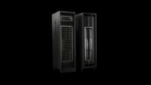
The GB200 NVL72 connects 36 GB200 Grace Blackwell Superchips (72 B200 GPUs + 36 Grace CPUs) in a liquid-cooled rack with a single 72-GPU NVLink domain that behaves like one giant GPU for software. The system uses direct-to-chip liquid cooling, with liquid running through manifolds and cold plates attached to the CPUs and GPUs in each compute tray.[9]
Physically, the GB200 NVL72 rack measures 600 mm wide by 1,068 mm deep by 2,236 mm high and weighs approximately 1.36 metric tons (3,000 pounds). System power consumption is approximately 120 to 132 kW, with 115 kW liquid-cooled and 17 kW air-cooled components.[9]
| Metric | GB200 NVL72 (rack) | GB200 Grace Blackwell Superchip (per node) |
|---|---|---|
| FP4 Tensor Core (with sparsity) | 1,440 PFLOPS | 40 PFLOPS |
| FP8/FP6 Tensor Core (with sparsity) | 720 PFLOPS | 20 PFLOPS |
| INT8 Tensor Core (with sparsity) | 720 POPS | 20 POPS |
| FP16/BF16 Tensor Core (with sparsity) | 360 PFLOPS | 10 PFLOPS |
| TF32 Tensor Core | 180 PFLOPS | 5 PFLOPS |
| FP32 | 5,760 TFLOPS | 160 TFLOPS |
| FP64 / FP64 Tensor Core | 2,880 TFLOPS | 80 TFLOPS |
| GPU Memory (HBM3e) | Up to 13.4 TB, 576 TB/s | Up to 372 GB, 16 TB/s |
| NVLink Bandwidth | 130 TB/s | 3.6 TB/s |
| CPU Cores (Arm Neoverse V2) | 2,592 | 72 |
| CPU Memory (LPDDR5X) | Up to 17 TB, up to 18.4 TB/s | Up to 480 GB, up to 512 GB/s |
GB200 NVL36x2
The GB200 NVL36x2 is an alternative rack configuration that splits the 72-GPU domain across two interconnected cabinets, each containing 18 Grace CPUs and 36 Blackwell GPUs. This configuration uses a hybrid cooling approach where the Grace CPUs, Blackwell GPUs, ConnectX-7 NICs, and NVLink Switch ASICs are liquid-cooled, while the remaining components are air-cooled. Power consumption is approximately 66 kW per rack (132 kW total for both racks), roughly 10 kW more than the NVL72 configuration due to additional NVSwitch ASICs and cross-rack interconnect cabling. The NVL36x2 uses 36 NVSwitch5 ASICs in total (compared to 18 in the NVL72) to maintain full-bisection NVLink bandwidth across the two cabinets.[9]
This configuration is expected to be the most commonly deployed form factor for GB200 systems, as it is compatible with a wider range of existing datacenter environments that may not support the density or cooling requirements of the single-rack NVL72.
Blackwell Ultra (GB300 Generation)
In March 2025 at GTC 2025, NVIDIA introduced "Blackwell Ultra," the B300 GPU and GB300 NVL72 system. The B300 GPU retains the dual-die Blackwell design with 208 billion transistors but increases the enabled SM count to 160 SMs total (yielding approximately 20,480 CUDA cores). It upgrades to 288 GB of HBM3e memory per GPU, supports PCIe Gen 6 host links at 256 GB/s bidirectional, integrates ConnectX-8 SuperNICs at 800 Gb/s per port, and draws 1,400 W of power.[10][20]
| Specification | B200 | B300 (Blackwell Ultra) |
|---|---|---|
| GPU Memory | 192 GB HBM3e | 288 GB HBM3e |
| Memory Bandwidth | 8 TB/s | 8 TB/s |
| NVFP4 / FP4 Dense Performance | 9 PFLOPS | 15 PFLOPS |
| NVFP4 / FP4 Sparse Performance | 20 PFLOPS | 30 PFLOPS |
| NVLink Bandwidth | 1.8 TB/s | 1.8 TB/s |
| Host Interface | PCIe Gen 5 | PCIe Gen 6 |
| TDP | 1,000 W | 1,400 W |
| CUDA Cores | ~18,432 | ~20,480 |
The GB300 NVL72 rack system delivers 1.5x more dense NVFP4 Tensor Core throughput and 2x higher attention-layer performance than the GB200 NVL72, with NVIDIA citing "50x higher AI factory output" relative to Hopper systems when efficiency, throughput, and latency are combined.[20] In MLPerf Training v5.0 / v5.1 benchmarks, the GB300 NVL72 demonstrated 1.9x faster training than the GB200 NVL72 at equivalent GPU scale, and 4.2x cumulative improvement over the H100 baseline. Blackwell Ultra products began shipping in the second half of 2025, with cloud providers including Microsoft, CoreWeave, and Oracle Cloud Infrastructure deploying production GB300 NVL72 systems at scale by late 2025.[10][22]
NVIDIA also announced the DGX Station with GB300 Grace Blackwell Superchip, a workstation-class system aimed at researchers and developers who need access to Blackwell Ultra performance without deploying full rack-scale infrastructure.
Consumer Products (GeForce RTX 50 Series)
The GeForce RTX 50 series based on Blackwell architecture was announced at CES 2025 on January 6, 2025. Consumer dies use TSMC 4N process and do not feature the dual-die design of datacenter parts. Consumer Blackwell GPUs include several features specific to gaming and content creation.[11]
Fourth-Generation RT Cores. Feature Triangle Cluster Intersection Engine for mega geometry and Linear Swept Spheres for rendering fine details like hair, with 2x ray-triangle intersection throughput compared to the previous generation.[2]
DLSS 4 and Multi Frame Generation. The RTX 50 series supports DLSS 4 with Multi Frame Generation, which can generate up to three additional frames per rendered frame, significantly boosting frame rates in supported games.
| Model | GPU | CUDA Cores | Memory | Bus Width | Die Size | Transistors | TDP | MSRP | Release Date |
|---|---|---|---|---|---|---|---|---|---|
| RTX 5090 | GB202-300-A1 | 21,760 | 32 GB GDDR7 | 512-bit | 750 mm2 | 92.2 bn | 575W | $1,999 | January 30, 2025 |
| RTX 5080 | GB203-200-A1 | 10,752 | 16 GB GDDR7 | 256-bit | 378 mm2 | 45.6 bn | 360W | $999 | January 30, 2025 |
| RTX 5070 Ti | GB203-300-A1 | 8,960 | 16 GB GDDR7 | 256-bit | 378 mm2 | 45.6 bn | 300W | $749 | February 2025 |
| RTX 5070 | GB205-300-A1 | 6,144 | 12 GB GDDR7 | 192-bit | 263 mm2 | 31.1 bn | 250W | $549 | February 2025 |
Professional RTX PRO Blackwell series includes RTX PRO 6000 (96 GB VRAM, April 2025) and RTX PRO 5000/4500/4000 (summer 2025).[13]
How does Blackwell compare to previous generations?
The following table compares the flagship datacenter GPUs across NVIDIA's three most recent architecture generations:
| Feature | NVIDIA H100 (Hopper) | NVIDIA H200 (Hopper) | NVIDIA B200 (Blackwell) |
|---|---|---|---|
| Transistors | 80 Billion | 80 Billion | 208 Billion (dual-die) |
| Process Node | TSMC 4N | TSMC 4N | TSMC 4NP |
| CUDA Cores | 14,592 | 14,592 | ~18,432 |
| Tensor Cores | 456 (4th gen) | 456 (4th gen) | 592 (5th gen) |
| Max AI Performance (Sparse) | 4 PFLOPS (FP8) | 4 PFLOPS (FP8) | 20 PFLOPS (FP4) / 10 PFLOPS (FP8) |
| Max GPU Memory | 80 GB HBM3 | 141 GB HBM3e | 192 GB HBM3e |
| Memory Bandwidth | 3.35 TB/s | 4.8 TB/s | 8 TB/s |
| NVLink (GPU-to-GPU) | 4th Gen: 900 GB/s | 4th Gen: 900 GB/s | 5th Gen: 1.8 TB/s |
| Lowest Supported Precision | FP8 | FP8 | FP4 |
| TDP | 700W | 700W | 1,000W |
| NVLink Domain (Max GPUs) | 256 | 256 | 576 |
The jump from H100 to B200 is particularly notable in memory capacity (2.4x), memory bandwidth (2.4x), and peak AI throughput at the lowest supported precision (5x at FP4 vs FP8). The transition from 80 billion to 208 billion transistors was enabled by the dual-die design, as no single die at current process nodes could accommodate that transistor count.
Training and Inference Performance
Training Benchmarks
Blackwell has demonstrated substantial improvements in AI training performance across multiple benchmarks. In MLPerf Training v5.0 and v5.1 submissions:
- The GB200 NVL72 achieved 3.2x faster training on the Llama 3.1 405B benchmark at 512 GPU scale compared to optimized Hopper submissions running FP8.[14]
- Compared to the H100, the B200 achieved 2.2x higher performance when fine-tuning Llama 2 70B and 2x higher performance when pre-training GPT-3 175B.[14]
- In the largest-scale test, a joint CoreWeave, NVIDIA, and IBM submission using 2,496 Blackwell GPUs completed Llama 3.1 405B training in 27.33 minutes, 2.1x faster than NVIDIA's own 2,560-GPU H100 submission.[14]
- Software optimizations between MLPerf v5.0 and v5.1 yielded an additional 1.4x performance improvement at similar GPU scale, demonstrating that Blackwell's performance continues to improve as NVIDIA refines its NVFP4 training recipes.[14]
- NVIDIA claims approximately 1.9x performance per dollar compared to H100 based on MLPerf training results and public GPU rental pricing.[14]
Inference Benchmarks
Blackwell's inference capabilities have been validated through MLPerf Inference v5.0 and v5.1 benchmarks. Selected v5.0 results on B200 8-GPU systems:
| Benchmark | B200 (8-GPU) | H200 (8-GPU) | Speedup |
|---|---|---|---|
| Llama 2 70B (server) | 98,443 tokens/s | ~32,800 tokens/s | 3.0x |
| Llama 2 70B (offline) | 98,858 tokens/s | ~35,300 tokens/s | 2.8x |
| Mixtral 8x7B (server) | 126,845 tokens/s | ~60,400 tokens/s | 2.1x |
| Mixtral 8x7B (offline) | 128,148 tokens/s | ~61,000 tokens/s | 2.1x |
| Stable Diffusion XL (server) | 28.44 samples/s | ~17.8 samples/s | 1.6x |
The GB200 NVL72 system demonstrated even more dramatic gains due to its unified 72-GPU NVLink domain. On the Llama 3.1 405B benchmark, the NVL72 delivered up to 30x higher throughput compared to an H200 NVL8 submission, achieving 3.4x higher per-GPU performance. This multiplied advantage comes from the fact that the 405B model can be distributed across all 72 GPUs without inter-node communication bottlenecks.[15]
In MLPerf Inference v5.1 (September 2025), the GB300 NVL72 made its debut and set records on the newly added DeepSeek-R1 671B mixture-of-experts reasoning model: 5,842 tokens/second/GPU in the offline scenario and 2,907 tokens/second/GPU in the server scenario, representing a 45% offline / 25% server improvement over the GB200 NVL72 per GPU and roughly 5x the throughput of unverified Hopper submissions. Submissions used NVFP4 acceleration, FP8 key-value cache quantization, expert parallelism for MoE routing, and disaggregated serving that decouples prompt prefill from token generation across separate GPU pools; disaggregated serving alone contributed ~1.5x throughput on Llama 3.1 405B interactive.[22]
NVIDIA's Performance Claims
At the original Blackwell announcement, NVIDIA stated that, per chip, Blackwell delivers:
- Up to 2.5x the FP8 training throughput of NVIDIA Hopper
- Up to 5x the inference performance at FP4
- 30x faster real-time trillion-parameter LLM inference (NVL72 vs H100 cluster)
- 4x faster LLM training at massive scale
- 25x improvement in cost and energy efficiency for trillion-parameter models
- 18x faster database query performance compared to CPUs[3][10]
NVIDIA's March 18, 2024 launch announcement framed the leap in the company's own words: "Blackwell GPU architecture features six transformative technologies for accelerated computing, which will help unlock breakthroughs in data processing, engineering simulation, electronic design automation, computer-aided drug design, quantum computing and generative AI."[3]
Power Consumption and Efficiency
Blackwell's power consumption represents a significant increase over previous generations, reflecting the architecture's focus on maximizing compute density:
| Product | TDP | Cooling Requirement |
|---|---|---|
| B100 | 700 W | Air-cooled (H100 compatible) |
| B200 | 1,000 W | Liquid cooling required |
| B300 (Blackwell Ultra) | 1,400 W | Liquid cooling required |
| DGX B200 (8-GPU system) | 10,200 W (system) | Liquid cooling for GPUs |
| GB200 NVL72 (rack) | 120,000 to 132,000 W | Direct-to-chip liquid cooling |
Despite the higher absolute power draw, NVIDIA claims a 25x improvement in energy efficiency per token for trillion-parameter model inference compared to the Hopper generation. This improvement stems from the combination of FP4 precision (which doubles throughput per watt relative to FP8), architectural efficiency gains in the Tensor Cores, and the reduced data movement overhead enabled by the NVLink domain architecture.[3]
In practice, measurements have shown that B200 GPUs often draw well below their 1,000 W TDP during typical inference workloads, with actual power consumption around 600 W for individual GPUs under moderate load. Training workloads that fully exercise the Tensor Cores push power consumption closer to the rated TDP.
How much does NVIDIA Blackwell cost?
Hardware Pricing
NVIDIA does not publish official retail prices for its datacenter GPUs, as they are sold through OEM partners and system integrators. However, early listings and OEM quotes provide approximate pricing:
| Product | Estimated Price |
|---|---|
| B200 192GB SXM (individual GPU) | $45,000 to $50,000 |
| DGX B200 (8-GPU server) | ~$515,000 |
| GB200 NVL72 (complete rack) | $2,000,000 to $3,000,000 (estimated) |
These prices are rough estimates and vary based on volume, configuration, and partner. By comparison, the H100 SXM GPU had an estimated street price of $25,000 to $40,000 at launch, though prices declined over 2024 and 2025 as supply improved.
Cloud Availability
All major cloud service providers have launched Blackwell-based instances:
| Cloud Provider | Instance/Offering | Configuration | Status (as of early 2026) |
|---|---|---|---|
| Amazon Web Services (AWS) | EC2 P6 instances, GB200 NVL72 | 8x B200 (P6), 72-GPU NVL72 | Generally available |
| Google Cloud | A4 VMs (HGX B200), A4X (GB200) | 8x B200 per VM | Generally available |
| Microsoft Azure | ND GB200 v6, NDv6 GB300 series | GB200 and GB300 NVL72 | Generally available |
| Oracle Cloud (OCI) | OCI Supercluster, OCI Compute | B200, GB200, GB300 | Generally available |
| CoreWeave | Blackwell clusters | GB200 / GB300 NVL72 racks | Generally available |
| Lambda | Cloud instances | 8x B200 / B300 | Generally available |
| Nebius | EU instances | GB300 NVL72 (Finland DC) | Generally available |
Cloud pricing for B200 GPUs varies significantly by provider and commitment level. On-demand pricing typically ranges from $5 to $7 per GPU-hour, while spot or preemptible instances can be as low as $2.25 per GPU-hour. Most providers offer B200s only in 8-GPU instances (matching the HGX B200 baseboard configuration), though some providers offer fractional GPU access through serverless platforms.[16]
Notable Deployments (2025-2026)
- Microsoft Azure / OpenAI (October 2025). Microsoft delivered the world's first at-scale production GB300 NVL72 cluster - the NDv6 GB300 VM series - with over 4,600 Blackwell Ultra GPUs connected via NVIDIA Quantum-X800 InfiniBand and engineered for OpenAI's frontier reasoning workloads. The cluster delivers 37 TB of fast memory and 1.44 EFLOPS of FP4 per VM.[23]
- xAI Colossus 2 (Memphis). Successor to the H100-based Colossus, scaling toward 500,000+ NVIDIA GPUs including Blackwell-class accelerators.[17]
- OpenAI / Oracle Stargate (Abilene, TX). Plans to deploy 64,000 GB200 GPUs by the end of 2026.[24]
- Nebius Finland. Europe's first operational production GB300 NVL72 deployment, online in early 2026.[25]
- AMAX DGX SuperPOD. 64-system DGX B200 SuperPOD with 512 Blackwell GPUs, 4.6 EFLOPS training / 9.2 EFLOPS inference, delivered for a leading generative AI developer.[26]
- Block, Inc. First North American DGX GB200 SuperPOD deployment announced 2024-2025.[27]
Is NVIDIA Blackwell sold out?
By November 2024, Morgan Stanley reported that the entire 2025 production of Blackwell was sold out. Major cloud providers including Amazon Web Services, Google, Meta, Microsoft, OpenAI, Oracle, and Tesla committed to adopting Blackwell-based systems.[2] By late 2025, press reports cited a backlog of roughly 3.6 million Blackwell units (B200 + GB200) sold out through mid-2026, and analysts estimated ~2 million Blackwell GPUs had been shipped into production.[17] In NVIDIA's Q1 FY2026 earnings (quarter ending April 28, 2025), Blackwell contributed nearly 70% of datacenter compute sales as the Hopper-to-Blackwell transition neared completion; in Q2 FY2026 (ending July 27, 2025), Blackwell datacenter revenue grew 17% sequentially against a total $46.7 billion quarterly revenue.[18][19]
Initial consumer RTX 50 series availability faced supply constraints, with some units found missing eight render output units (ROPs) due to a "production anomaly" affecting less than 0.5% of cards according to NVIDIA.[15]
Software, Networking, and Platforms
Blackwell systems are offered in HGX and DGX platforms, and as managed DGX Cloud instances. They pair with NVIDIA's Quantum-X800 InfiniBand and Spectrum-X Ethernet fabrics (up to 800 Gb/s) and BlueField-3 DPUs for secure, composable acceleration.[3] Blackwell Ultra systems additionally integrate ConnectX-8 SuperNICs at 800 Gb/s per port.[20]
For inter-node networking, Blackwell systems support both InfiniBand and Ethernet-based fabrics:
- Quantum-X800 InfiniBand: NVIDIA's latest InfiniBand fabric delivers 800 Gb/s per port, optimized for AI training workloads that require low-latency collective operations across hundreds or thousands of GPUs.
- Spectrum-X800 Ethernet: An alternative for organizations that prefer Ethernet-based networking, Spectrum-X provides similar bandwidth with features like adaptive routing and congestion control tuned for AI workloads.
- BlueField-3 DPU: Data processing units that offload networking, storage, and security functions from the host CPU, enabling more efficient multi-tenant GPU sharing in cloud environments.
NVIDIA AI Enterprise includes NVIDIA NIM inference microservices for Blackwell deployment, and the TensorRT-LLM library provides optimized kernels that take advantage of Blackwell's FP4 / NVFP4 Tensor Cores. Open-source serving stacks including SGLang and vLLM ship native NVFP4 kernels for Blackwell Ultra. The CUDA compute capability for Blackwell datacenter GPUs is 10.0 (Blackwell) and 12.0 (Blackwell Ultra), with CUDA 12.8+ required for full support.[1][20]
Future Roadmap
NVIDIA maintains an aggressive annual release cadence for its datacenter GPU architectures:
| Year | Architecture | Key Product | Process | Memory |
|---|---|---|---|---|
| 2022 | Hopper | H100 | TSMC 4N | HBM3 |
| 2023 | Hopper (refresh) | H200 | TSMC 4N | HBM3e |
| 2024 | Blackwell | B200 / GB200 | TSMC 4NP | HBM3e |
| 2025 | Blackwell Ultra | B300 / GB300 | TSMC 4NP | HBM3e |
| 2026 | Vera Rubin | Rubin NVL144 | TSMC 3 nm class | HBM4 |
| 2027 | Rubin Ultra | Rubin Ultra NVL576 (Kyber) | TSMC 3 nm class | HBM4e |
| 2028+ | Feynman | TBD | TBD | TBD |
At CES January 2026, NVIDIA confirmed that Vera Rubin had entered full production. The Rubin platform spans six chips co-designed end-to-end: the Vera CPU (88 custom NVIDIA "Olympus" Armv9.2 cores), the Rubin GPU (two reticle-sized dies, ~50 PFLOPS of dense NVFP4 with a third-generation Transformer Engine), the NVLink 6 Switch (3.6 TB/s per GPU; 260 TB/s aggregate per NVL72 rack), the ConnectX-9 SuperNIC, the BlueField-4 DPU, and the Spectrum-6 Ethernet Switch.[28] The Vera Rubin NVL144 packs 144 Rubin GPU dies (72 packages) with 36 Vera CPUs to deliver up to 3.6 EFLOPS of NVFP4 inference and 1.2 EFLOPS of FP8 training, paired with HBM4 memory. Volume Rubin shipments target the second half of 2026, with AWS, Google Cloud, Microsoft, OCI, and CoreWeave among the first adopters; NVIDIA cites up to 5x inference and 3.5x training improvements over Blackwell, and 10x lower cost per token.[28]
Rubin Ultra (2027) doubles per-package compute by moving to a four-reticle GPU configuration delivering ~100 PFLOPS of NVFP4 with up to 1 TB of HBM4e per package across 16 HBM sites. The Rubin Ultra NVL576 "Kyber" rack rotates compute blades into a vertical orientation, packing 576 GPU dies into a single ~600 kW rack - roughly 5x current rack power. After Rubin, NVIDIA's next datacenter architecture will be named after theoretical physicist Richard Feynman.[28]
See also
- NVIDIA RTX Spark
- Volta (microarchitecture)
- ChipNeMo
- NVIDIA DGX Station for Windows
- NVIDIA RTX Spark
- NVIDIA Hopper
- Ada Lovelace (microarchitecture)
- Grace CPU
- NVLink
- GeForce RTX 50 series
- Tensor Core
- David Blackwell
- DGX SuperPOD
- DLSS
- GPU Computing
- Deep Learning
- Large Language Model
Recent developments (2026)
On February 25, 2026, NVIDIA reported results for the fourth quarter of fiscal 2026 (quarter ended January 25, 2026) that the company attributed largely to Blackwell demand. Quarterly revenue reached a record $68.1 billion, up 20% sequentially and 73% year over year, while data center revenue hit a record $62.3 billion, up 22% sequentially and 75% year over year. Full-year fiscal 2026 revenue was $215.9 billion (up 65%), with full-year data center revenue of $193.7 billion (up 68%). GAAP and non-GAAP gross margins for the quarter were 75.0% and 75.2%. NVIDIA guided Q1 fiscal 2027 revenue to $78.0 billion plus or minus 2% (with GAAP gross margin of 74.9%), assuming no China data center compute revenue. CEO Jensen Huang said "Grace Blackwell with NVLink is the king of inference today, delivering an order-of-magnitude lower cost per token, and Vera Rubin will extend that leadership even further," and the company stated that Blackwell Ultra delivers up to 50x better performance and 35x lower cost for agentic AI compared with the Hopper platform.[29][30]
At GTC 2026, held March 16 to 19, 2026 in San Jose, Huang told the keynote audience that he saw "at least $1 trillion" in cumulative orders for Blackwell and Vera Rubin systems through 2027. That figure roughly doubled the approximately $500 billion in Blackwell-and-Rubin demand through 2026 that he had cited at the prior year's GTC, and it framed Blackwell and Blackwell Ultra as the volume products bridging to the Rubin generation, which NVIDIA reiterated it expects to ramp in the second half of 2026.[31][32]
Through the first half of 2026, GB300 NVL72 (Blackwell Ultra) racks moved into broader volume production across OEMs including Dell, Lenovo, and Quanta. Dell had delivered the market's first GB300 NVL72 system to CoreWeave in mid-2025, and additional partners brought GB300 platforms to market through 2026.[33]
References
- NVIDIA Blackwell Architecture Technical Overview. NVIDIA. 2024. ↩
- Blackwell (microarchitecture)). Wikipedia. ↩
- NVIDIA Blackwell Platform Arrives to Power a New Era of Computing. NVIDIA Newsroom. March 18, 2024. ↩
- David Blackwell. Wikipedia. ↩
- The Engine Behind AI Factories: NVIDIA Blackwell Architecture. NVIDIA. ↩
- NVIDIA Secure AI with Blackwell and Hopper GPUs Whitepaper. NVIDIA. 2025. ↩
- GB200 NVL72. NVIDIA. ↩
- DGX B200: The Foundation for Your AI Factory. NVIDIA. ↩
- GB200 NVL72 Deployment: Managing 72 GPUs in Liquid-Cooled Configurations. Introl. 2024. ↩
- NVIDIA Blackwell Ultra AI Factory Platform Paves Way for Age of AI Reasoning. NVIDIA Newsroom. March 2025. ↩
- GeForce RTX 50 Series. NVIDIA. January 2025. ↩
- Who is David Blackwell?. HPCwire. March 22, 2024.
- NVIDIA RTX PRO Blackwell Series. NVIDIA. 2025. ↩
- NVIDIA Blackwell Enables 3x Faster Training and Nearly 2x Training Performance Per Dollar. NVIDIA Developer Blog. ↩
- NVIDIA Blackwell Delivers Massive Performance Leaps in MLPerf Inference v5.0. NVIDIA Developer Blog. ↩
- How much does it cost to run NVIDIA B200 GPUs in 2025?. Modal Blog. ↩
- Nvidia's Blackwell Dynasty: B200 and GB200 Sold Out Through Mid-2026 as Backlog Hits 3.6 Million Units. FinancialContent. December 2025. ↩
- NVIDIA Announces Financial Results for First Quarter Fiscal 2026. NVIDIA. May 2025. ↩
- NVIDIA Announces Financial Results for Second Quarter Fiscal 2026. NVIDIA. August 2025. ↩
- Inside NVIDIA Blackwell Ultra: The Chip Powering the AI Factory Era. NVIDIA Developer Blog. 2025. ↩
- NVIDIA DGX B300: An AI Factory for AI Reasoning. NVIDIA. ↩
- NVIDIA Blackwell Ultra Sets New Inference Records in MLPerf Debut. NVIDIA Developer Blog. September 2025. ↩
- Microsoft Azure Unveils World's First NVIDIA GB300 NVL72 Supercomputing Cluster for OpenAI. NVIDIA Blog. October 2025. ↩
- Block, Inc. to deploy Nvidia DGX SuperPod with GB200s. Data Center Dynamics. ↩
- Nebius delivers Europe's first live NVIDIA GB300 NVL72 deployment. Nebius. 2026. ↩
- AMAX Deploys NVIDIA DGX SuperPOD with 512 Blackwell GPUs for GenAI Developer. HPCwire. 2025. ↩
- DGX SuperPOD: AI Infrastructure for Enterprise Deployments. NVIDIA. ↩
- NVIDIA Kicks Off the Next Generation of AI With Rubin: Six New Chips, One Incredible AI Supercomputer. NVIDIA Newsroom. January 2026. ↩
- NVIDIA Announces Financial Results for Fourth Quarter and Fiscal 2026. NVIDIA Newsroom. February 25, 2026. ↩
- Nvidia smashes Q4 2026 with $68 billion in revenue, and a Q1 outlook that quashes AI bubble talk. Fortune. February 25, 2026. ↩
- Nvidia GTC 2026: CEO Jensen Huang sees $1 trillion in orders for Blackwell and Vera Rubin through '27. CNBC. March 16, 2026. ↩
- Jensen just put Nvidia's Blackwell and Vera Rubin sales projections into the $1 trillion stratosphere. TechCrunch. March 16, 2026. ↩
- Dell Delivers Market's First NVIDIA GB300 NVL72 to CoreWeave. Dell. 2026. ↩
Improve this article
Add missing citations, update stale details, or suggest a clearer explanation. Every suggestion is reviewed for sourcing before it goes live.
13 revisions by 1 contributors · full history